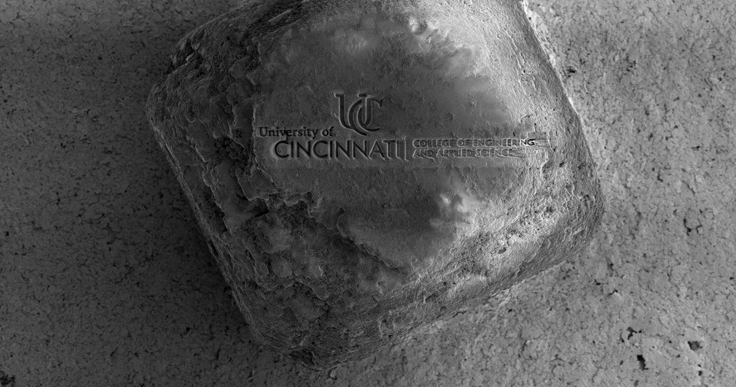
UC's Advanced Materials Characterization Center used a dual-beam scanning electron microscope to carve UC's logo into a grain of salt. (Photo by Melodie Fickenscher.)
Etch UC's logo onto a grain of salt?
No prob.
Technology at UC's Advanced Materials Characterization Center enables scientists to study the smallest objects.
By Michael Miller
513-556-6757
Photos by Andrew Higley/UC Creative Services
May 16, 2017
To solve a problem, first you have to see it, either metaphorically or literally.
The University of Cincinnati invested in a scientific instrument last year to give researchers a closer look at everything from industrial samples to nanowire a thousand times smaller than a human hair.
UC’s $1.4 million dual-beam scanning electron microscope has become an all-purpose tool for students, researchers and even private industry to study problems up close.
“It’s the only way to see it,” said Melodie Fickenscher, director of the Advanced Materials Characterization Center in the College of Engineering and Applied Science.
“It” could be a crack in a weld or a gap in a circuit or the beautiful symmetry of a fruit fly’s eye. Under such intense magnification, grains of pollen suddenly become scaled dragon’s eggs while spiders take on the proportions of movie-screen monsters.
"Physicists use it, biologists use it, doctors use it. It’s invaluable for research."
‒ Melodie Fickenscher, director of UC's Advanced Materials Characterization Center
The center has four powerful microscopes, including a state-of-the-art machine UC purchased last year. Among them is a transmission electron microscope from 1989 with a faded yellow computer case and a green monitor that looks like a prop from the Matthew Broderick movie “WarGames.”
All generate vivid images that could not be obtained any other way, even if the older model originally required the technicians to process photo film.
“You never knew if you got the shot until you developed the film,” Fickenscher said.
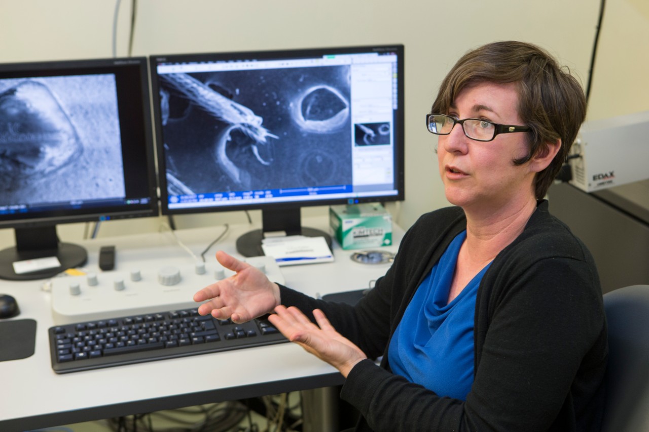
Melodie Fickenscher, director of UC's Advanced Materials Characterization Center, uses microscopy to help businesses solve production problems.
The scanning electron microscope shoots a beam of electrons at the sample and measures the resulting intensity of the signals at each point to render a grayscale black-and-white image. The image can be manipulated by the operator to improve resolution or contrast.
“This is part of a $20 bill that my dog ate,” Fickenscher said, zooming in to show how the machine can differentiate trace metals from the linen fibers that make up an American bill.
“Physicists use it, biologists use it, doctors use it. It’s invaluable for research,” she said.
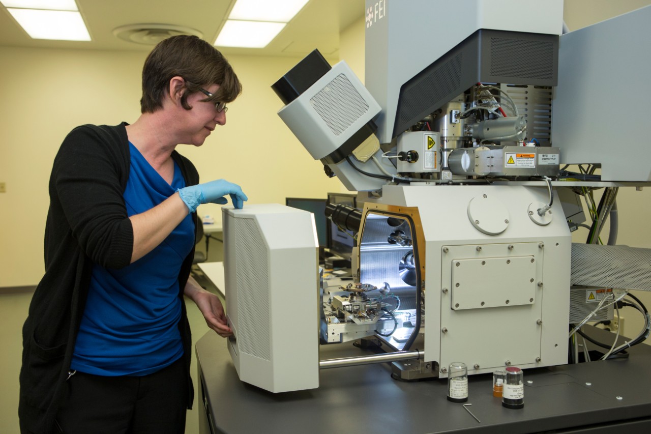
Fickenscher opens a dual-beam scanning electron microscope to study a sample.
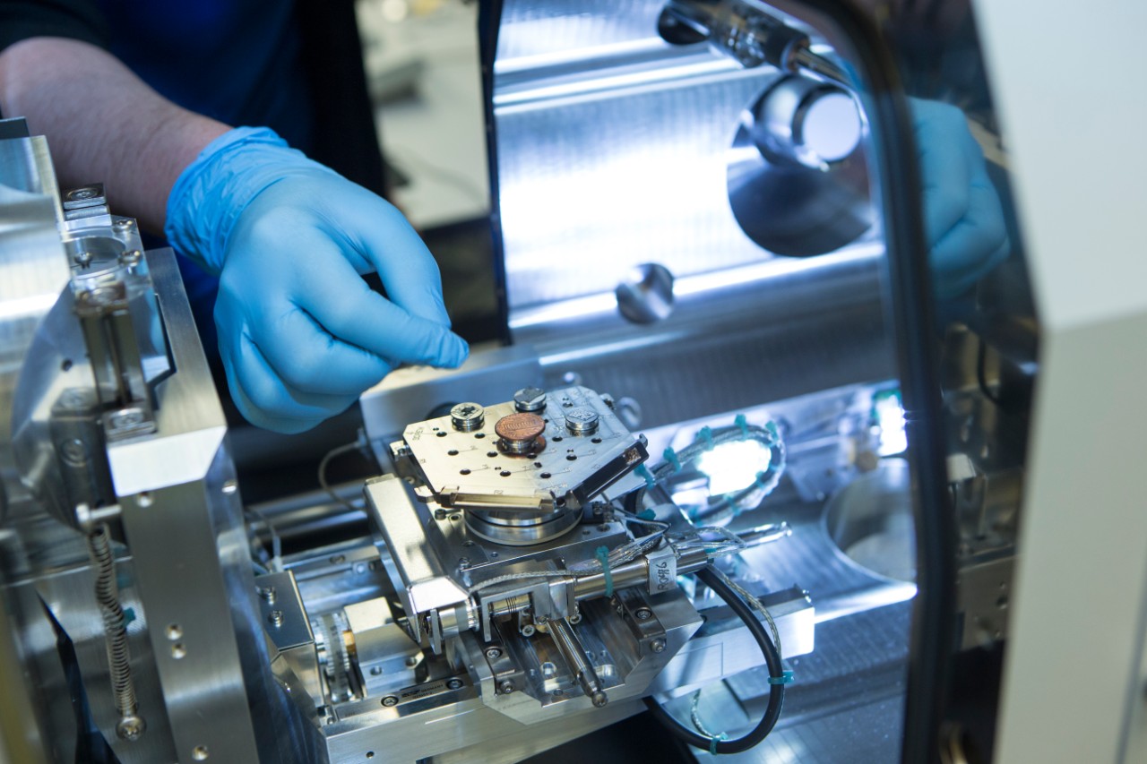
A penny is placed in the electron microscope for a demonstration at UC's Advanced Materials Characterization Center.
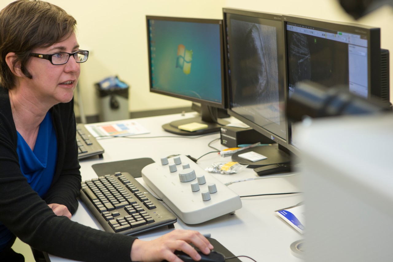
Fickenscher uses a computer to render images of a sample.
A fast scan renders an image so quickly that it gives the illusion of viewing the sample in real time, like moving a glass slide under an optical microscope. But getting finer resolution takes longer as the electron beam scans back and forth across the sample, building an image like a dot-matrix printer.
Dual-beam microscopes have the added ability to fire gallium ions at a sample to create a cross-section or etch away layers of material such as tissue or metal. The lab used this tool to carve UC’s logo into a grain of salt as a demonstration.
Students and professors in a variety of science fields use the microscopes: from engineers and chemists to biologists and physicists. Even students at UC’s College of Design, Architecture, Art, and Planning have created novel art projects with its images.
"The new scanning electron microscope helps us further optimize our products. It provides a very powerful analytical result.”
‒ Danqing Zhu, principal scientist at Ecosil Technologies
“It’s an amazing technology,” said Vesselin Shanov, a professor in the College of Engineering and Applied Science.
He recently used both kinds of microscope to examine carbon nanotubes.
“We wanted to learn more about their properties, including their structure. The nanotubes self-assemble in vertically aligned arrays when we synthesize them,” Shanov said. “The best way to look at their internal structure was by cutting a tiny piece of these arrays using a focused ion beam and extracting it for further observation with high-resolution scanning and transmission electron microscopes.”
The microscope also gets a lot of attention from Cincinnati-area industry. UC leases out the microscope to businesses that want a closer look at parts or products.
“You can do failure analysis. If you had a failed circuit you could etch away the top layer and look at what shorted out underneath it,” Fickenscher said.

A sweat bee. (Wikimedia Commons/Judy Gallagher)
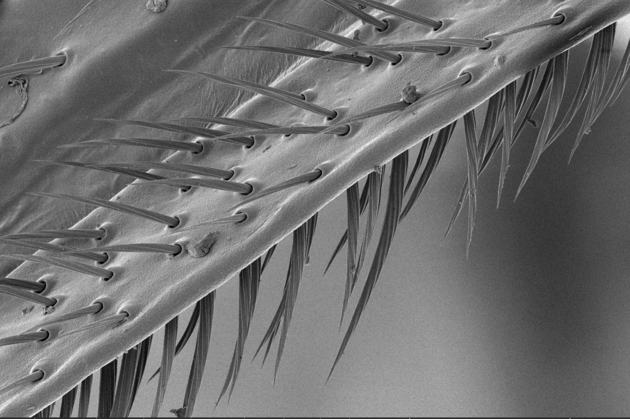
The hairs of a bee's leg magnified with a scanning electron microscope. (Photo by Melodie Fickenscher)

A pillbug. (Wikimedia Commons/Brian Gratwicke)
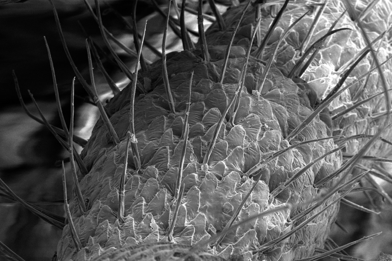
Microscopic examination reveals fine hairs and scales on the pillbug. (Photo by Melodie Fickenscher.)
The microscope’s elemental analyses can help companies solve problems, saving time and money in refining their industrial processes. For example, a company might try to determine how its parts or products are getting contaminated in production. Identifying the foreign properties is the first step to solving how the contamination happened, she said.
But Fickenscher said she can’t get into too many specifics.
“So much of the work I do is proprietary. So I can’t put it on the website or social media or talk about it,” she said.
Ecosil Technologies, based in Fairfield, Ohio, has used the scanning electron microscope to examine some of its coating products. The company develops innovative methods to adhere paints and sealants to metals in products as diverse as new cars or refrigerators.
“With the new microscope, you can clearly see any defects,” said Danqing Zhu, a UC doctoral graduate (CEAS ’05) and Ecosil’s principal scientist.
The microscopic images combined with other analyses help the company make modifications or improvements, she said.
“The new scanning electron microscope helps us further optimize our products,” she said. “It provides a very powerful analytical result.”
Fickenscher first used the university’s old electron microscope while studying nanowires as a physics graduate student.
"I liked doing this a lot more than doing physics," she said.
She pored over the manuals and soon became the university’s expert in the equipment, which requires both technical skills and an artistic sensibility.
“I have to adjust the brightness and contrast on this. Just like in photography, you have to try to get the balance right,” she said. “You can enhance the images in Photoshop to add color, but I’m a purist."
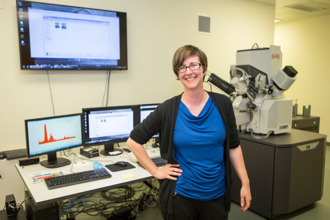
Melodie Fickenscher, director of UC's Advanced Materials Characterization Center, started her work at UC in the Physics Department.
Try it yourself
UC's Advanced Materials Characterization Center leases its equipment to students, staff and local businesses. Contact the center at 513-556-3220 for details.

