The magic of nanotechnology
UC physicists experiment with nanowire in a promising field that could make electronics smaller, faster and cheaper.
By Michael Miller
513-556-6757
Photos by Andrew Higley/UC Creative Services
March 15, 2017
In electronics, the race for smaller is huge.
Physicists at the University of Cincinnati are working to harness the power of nanowires, microscopic wires that have the potential to improve solar cells or revolutionize fiber optics.
Nanotechnology has the potential to solve the bottleneck that occurs in storing or retrieving digital data – or could store data in a completely new way.
UC professors and their graduate students presented their research at the March 13 conference of the American Physical Society in New Orleans, Louisiana.
Hans-Peter Wagner, associate professor of physics, and doctoral student Fatemesadat Mohammadi are looking at ways to transmit data with the speed of fiber optics but at a significantly smaller scale.
Wagner and lead author Mohammadi are studying this field, called plasmonics, with researchers from three other universities. For the novel experiment, they built nanowire semiconductors with organic material, fired laser pulses at the sample and measured the way light traveled across the metal; technically, the excitations of plasmon waves.
“So, if we succeed in getting a better understanding about the coupling between the excitations in semiconductor nanowires and metal films, it could open up a lot of new perspectives,” Wagner said.
The successful harnessing of this phenomenon -- called plasmon waveguiding -- could allow researchers to transmit data with light at the nano level.
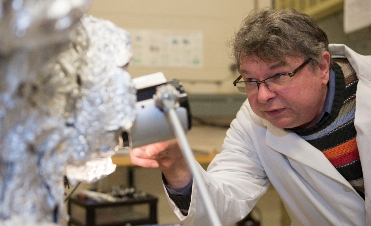
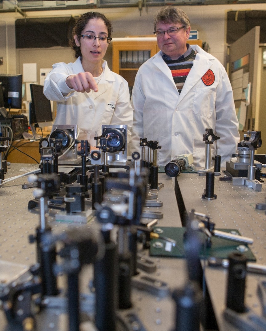
UC physicists such as Associate Professor Hans-Peter Wagner are exploring nanowire semiconductors to harness the power of light at the nano level.
Universities around the world are studying nanowires, which have ubiquitous applications from biomedical sensors to light-emitting diodes or LEDs. Four UC papers on the topic are among more than 150 others by nanowire researchers around the world to be presented at the March conference.
“You’re trying to optimize the physical structure on something approaching the atomic scale. You can make very high efficiency devices like lasers,” said Leigh Smith, head of UC’s Department of Physics.
Smith and UC Physics Professor Howard Jackson also presented papers on nanowires at the conference.
Virtually everyone benefits from this line of research, even if the quantum mechanics underlying the latest biosensors exceed a casual understanding. For example, home pregnancy tests use gold nanoparticles – the indicator that turns color.
“People use technologies all the time that they don’t understand,” Smith said. “Arthur C. Clarke said, ‘Any sufficiently advanced technology is indistinguishable from magic.’”
Gordon Moore, co-founder of Intel Corp., observed that the number of transistors used in a microchip has roughly doubled every two years since the 1970s. This phenomenon, now called Moore’s Law suggests that computer processing power improves at a predictable rate.
Some computer scientists predicted the demise of Moore’s Law was inevitable with the advent of microprocessors. But nanotechnology is extending that concept’s lifespan, said Brian Markwalter, senior vice president of research and technology for the Consumer Technology Association. His trade group represents 2,200 members in the $287 billion U.S. tech industry.
“It’s not a race to be small just to be the smallest. There’s a progression of being able to do more on smaller chips. The effect for consumers is that every year they get better and better products for the same price or less,” he said.
Nanotechnology is opening a universe of new possibilities, Markwalter said.
“It’s almost magical. They get better, faster, cheaper and use less power,” he said.
Markwalter said UC professor Wagner’s research is exciting because it shows promise in using optical switches to address a bottleneck in data transmission that occurs whenever you try to store or remove data.
“It’s really a breakthrough area to merge the semiconductor world and the optical world,” Markwalter said. “[Wagner’s] working at the intersection of fiber optics and photonics.”
But even nanotechnology has its limits, Smith said.
“We’re running toward the limits of what’s physically possible with present technologies,” Smith said. “The challenges are pretty immense. In 10 or 20 years there has to be a fundamental paradigm shift in how we make structures. If we don’t we’ll be caught at the same place we are now.”
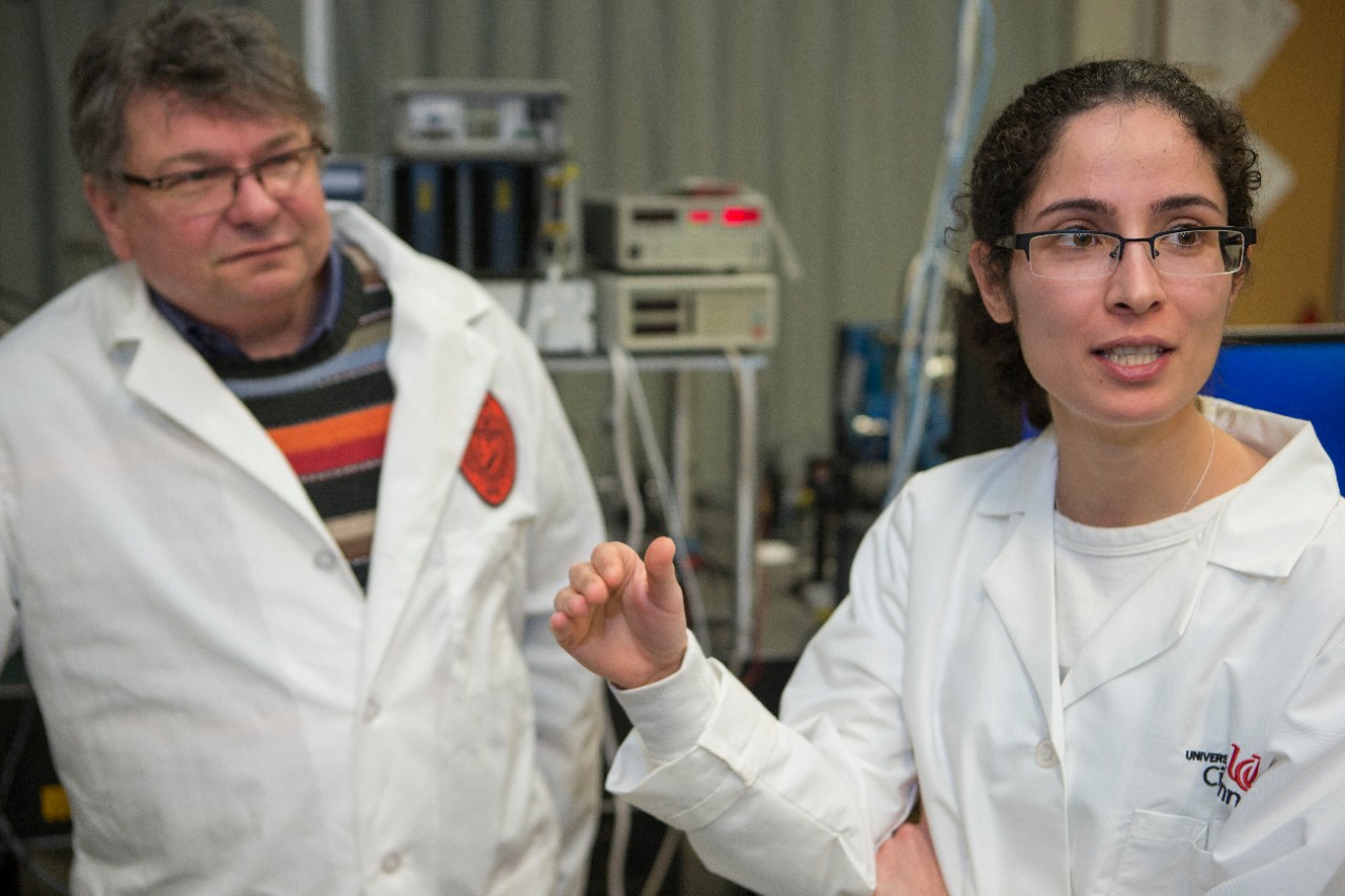
UC graduate student Fatemesadat Mohammadi and Associate Physics Professor Hans-Peter Wagner fire laser pulses at semiconductor nanowires to excite electrons (called excitons) that potentially serve as an energy pump to guide plasmon waves over a coated metal film just a few nanometers thick without losing power, a nettlesome physical property called resistivity
They measure the resulting luminescence of the nanowire to observe how light couples to the metal film. By sending light over a metal film, a process called plasmonic waveguiding, researchers one day could transmit data with light at the nano level.
“The luminescence is our interest. So we coat them and see: How does the photoluminescence characteristic change?” Mohammadi said.
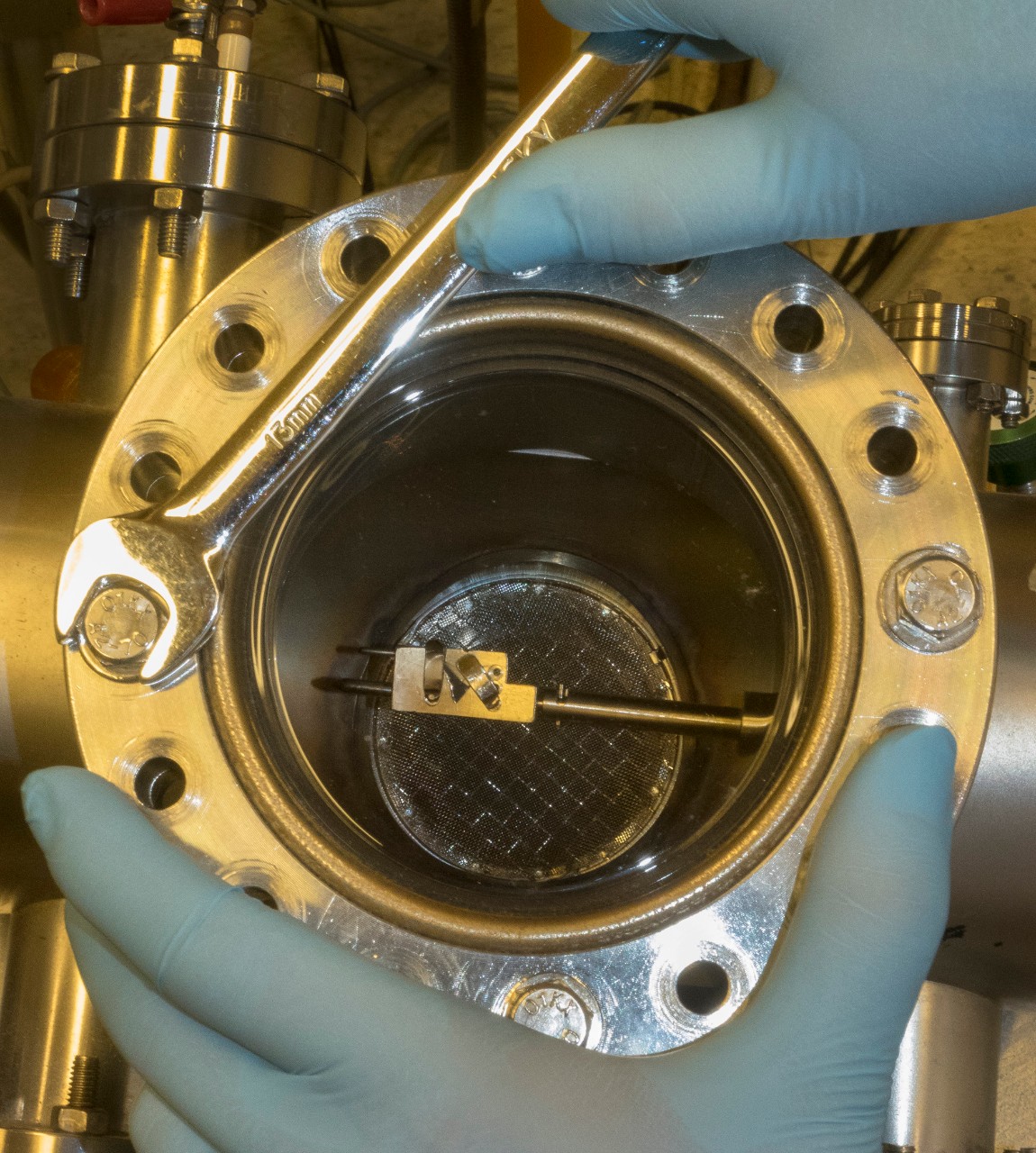
To make the semiconductor, they use a technique called high-vacuum organic molecular beam deposition (pictured above) to spread organic and metal layers on gallium-nitride nanorods.
The use of organic film is unique to the UC experiment, Wagner said. The film works as a spacer to control the energy flow between excitons in the nanowire and the oscillation of metal electrons called plasmons.
The organic material has the added benefit of also containing excitons that, arranged properly, could support the energy flow in a semiconductor, he said.
Coating the nanorods with gold significantly shortens the lifetime of the exciton emission resulting in what’s called a quenched photoluminescence. But by using organic spacers between the nanorod and the gold film, the researchers are able to extend the emission lifetime to nearly the equivalent of nanorods without a coating.
Once the gold-coated sample is prepared, they take it to an adjacent lab room and subject it to pulses of laser light.
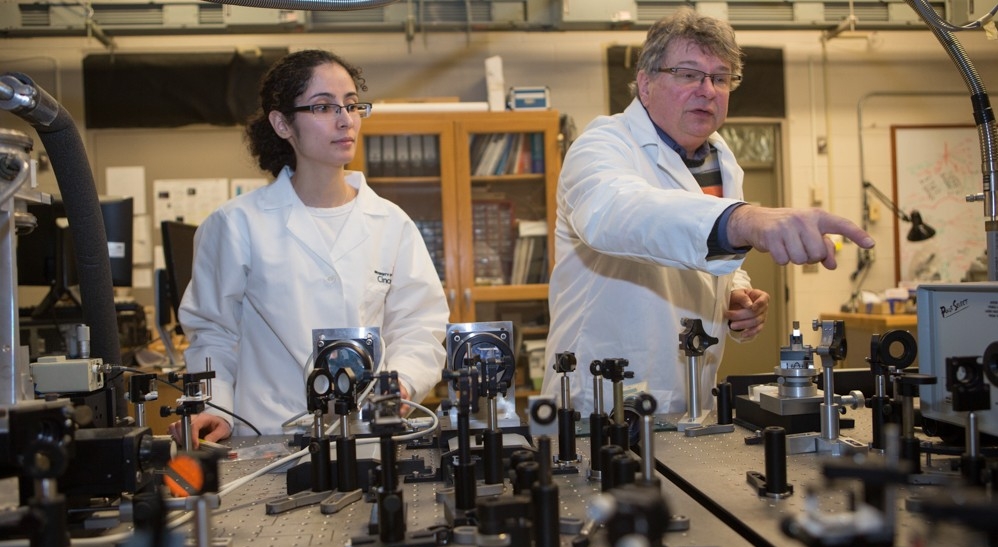
Mohammadi said it took days of painstaking work to arrange the small city of mirrors and beam splitters bolted at precise angles to a workbench for the experiment (pictured above left).
The reactions in the nanowire take just 10 picoseconds (which is a trillionth of a second.) And the laser pulses are faster still — 20 femtoseconds (a figure that has 15 zeros following it or a quadrillionth of a second.)
The UC project used a gold coating so that experiments could be replicated at a later date without risk of oxidation. But traditional coatings such as silver, Mohammadi said, hold even more promise.
Interested in physics? Apply to UC's undergraduate physics program or explore other programs on the undergraduate or graduate level.